There are two primary types of semiconductor materials: Intrinsic (pure) and Extrinsic (doped). While intrinsic semiconductors consist of a single element like Silicon, extrinsic semiconductors are categorized into N-type and P-type based on the specific doping process used to modify their electrical conductivity for modern chip design and high-frequency electronic applications.
Introduction
In the rapidly evolving landscape of 2026 electronics, semiconductors remain the fundamental building blocks of everything from quantum processors to electric vehicle (EV) power inverters. For electronics engineers and ECE students, understanding the various types of semiconductor materials is not merely an academic requirement it is a practical necessity for device characterization and circuit design.
This guide provides a comprehensive breakdown of semiconductor classifications, the physics of charge carriers, and the advanced manufacturing techniques used to manipulate these materials at the atomic level. We will examine why pure silicon is often insufficient for modern needs and how “controlled impurities” serve as the engine of the digital age.
How Many Types of Semiconductors Are There?
When addressing the question of how many types of semiconductors are there, we must look at them through the lens of material purity and chemical composition.
The Fundamental Split: Intrinsic vs. Extrinsic
At the most basic level, semiconductors are classified by their purity:
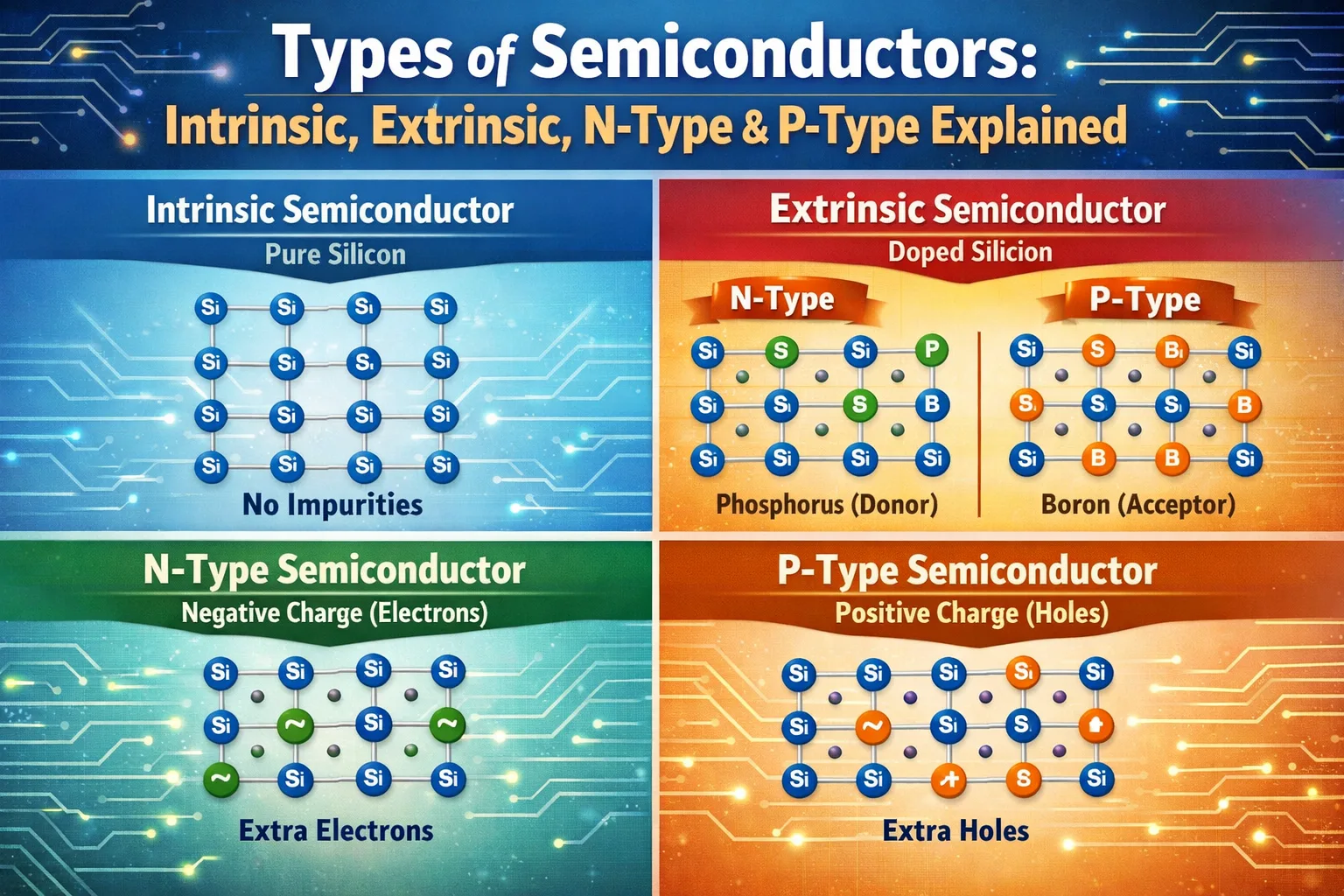
- Intrinsic Semiconductors: These are chemically pure materials without any significant presence of foreign atoms. In a perfect intrinsic crystal, every atom is of the same type (e.g., pure Silicon or Germanium).
- Extrinsic Semiconductors: These are “doped” materials. By intentionally introducing a small, controlled amount of impurity atoms into an intrinsic base, engineers can increase the conductivity by several orders of magnitude.
The Compositional Split: Elemental vs. Compound
Engineers also categorize what are the types of semiconductor materials based on their atomic makeup:
- Elemental Semiconductors: Found in Group IV of the periodic table, such as Silicon (Si) and Germanium (Ge).
- Compound Semiconductors: Formed by combining elements from different groups, such as Gallium Arsenide (GaAs) from Groups III and V, or Silicon Carbide (SiC) from Group IV.
Intrinsic Semiconductors: The Pure State
Intrinsic semiconductors serve as the starting point for all semiconductor device fabrication. In these materials, the number of free electrons ($n$) is always equal to the number of holes ($p$). This balance is known as the intrinsic carrier concentration ($n_i$).
$$n = p = n_i$$
At room temperature, thermal energy ($k T$) is sufficient to break a small number of covalent bonds, allowing electrons to jump from the valence band to the conduction band. However, for most engineering applications, the intrinsic conductivity of silicon is far too low to be useful in a circuit. This leads us to the necessity of extrinsic modification.
Extrinsic Semiconductors: N-Type and P-Type
The limitations of pure silicon are overcome through doping. This process creates extrinsic semiconductors, which are the “active” versions used in transistors and diodes.
Which Type of Doping Takes Place in N-Type Semiconductors?
If you are specifically looking for which type of doping take place in n-type semiconductor materials, the answer is pentavalent doping.
In an N-type semiconductor, atoms from Group V (Pentavalent elements) are added to the Silicon lattice. Common examples include:
- Phosphorus (P)
- Arsenic (As)
- Antimony (Sb)
These atoms have five valence electrons. When integrated into a Silicon lattice (which has four valence electrons), four of the dopant’s electrons form covalent bonds. The fifth electron is weakly bound and easily detached by thermal energy, becoming a “free” carrier. Because the material now has an abundance of negatively charged electrons, it is called “N-type” (Negative).
P-Type Semiconductors and Trivalent Doping
P-type semiconductors are created via trivalent doping (Group III elements). Examples include:
- Boron (B)
- Aluminum (Al)
- Gallium (Ga)
These atoms have only three valence electrons. When they replace a Silicon atom, they create a “vacancy” or a hole. In semiconductor physics, we treat this hole as a mobile positive charge carrier. Since holes are the majority carriers here, the material is “P-type” (Positive).
How Doping Works: The Step-by-Step Mechanism
The transition from an insulator-like state to a high-conductivity state follows a precise logical sequence. Here is how the atomic shift occurs during fabrication:
- Lattice Integration: Impurity atoms are introduced into the Silicon melt (during ingot growth) or through high-energy ion implantation on a wafer surface.
- Covalent Displacement: The dopant atom (e.g., Phosphorus) takes the place of a Silicon atom in the crystal lattice structure.
- Charge Carrier Release:
- In N-type: The 5th valence electron is “donated” to the conduction band.
- In P-type: An electron is “accepted” from the valence band, leaving a mobile hole behind.
- Energy State Alteration: The presence of these atoms creates new energy levels (Donor or Acceptor levels) just below the conduction band or just above the valence band, respectively.
Pro-Tip: Precision is everything. Doping concentrations can range from one dopant atom per $10^{10}$ silicon atoms to one per $10^3$. Even a tiny variation can change a transistor from a “switch” to a “short circuit.”
Technical Deep Dive: Energy Band Theory & Fermi Levels
To truly understand the types of semiconductor, an engineer must look at the energy band diagram.
The Fermi Level ($E_f$)
The Fermi level represents the probability (50%) of finding an electron at a specific energy state.
- In an Intrinsic semiconductor, the Fermi level lies almost exactly in the middle of the bandgap ($E_g$).
- In an N-type semiconductor, the addition of donor atoms shifts the Fermi level upward, closer to the Conduction Band ($E_c$).
- In a P-type semiconductor, the acceptor atoms pull the Fermi level downward, closer to the Valence Band ($E_v$).
The Law of Mass Action
One of the most critical equations for semiconductor professionals is the Law of Mass Action. It states that for a semiconductor in thermal equilibrium, the product of the electron and hole concentrations is a constant:
$$n \cdot p = n_i^2$$
This means that if you increase the number of electrons through N-type doping, the number of holes must decrease proportionally. This relationship is vital when calculating the base or collector currents in Bipolar Junction Transistors (BJTs).
Manufacturing: How We Create Doped Semiconductors
Creating the different types of semiconductor is a marvel of modern manufacturing. It involves several high-precision steps:
The Czochralski (CZ) Method
Most silicon starts as a “seed crystal” dipped into molten silicon. As the seed is slowly rotated and pulled, it forms a large, single-crystal ingot. If an N-type wafer is needed, the dopant (like Phosphorus) is added directly to the melt.
Ion Implantation
For modern microchips, where we need P-type and N-type regions side-by-side (such as in a CMOS transistor), we use Ion Implantation. High-energy ions of the dopant element are fired into specific areas of the wafer. This is followed by Annealing, a heating process that repairs the crystal lattice and “activates” the dopants.
Compound Semiconductors: The 2026 Frontier (SiC and GaN)
While Silicon is the most common, it is reaching its physical limits. Engineers are increasingly turning to Wide Bandgap (WBG) semiconductors.
- Silicon Carbide (SiC): Ideal for high-voltage applications. SiC-based power inverters are the reason modern EVs can charge faster and drive further.
- Gallium Nitride (GaN): Exceptional for high-frequency applications. You will find GaN in 5G base stations and the “fast chargers” used for laptops and smartphones.
These compound materials offer higher thermal conductivity and can operate at much higher temperatures than traditional silicon-based types of semiconductor.
Manufacturing & Advanced Materials (SiC & GaN)
Most silicon starts via the Czochralski (CZ) Method, where a seed crystal is pulled from molten silicon. However, Silicon is reaching its limits.
Wide Bandgap (WBG) Semiconductors
In 2026, the industry is shifting toward Compound Semiconductors:
- Silicon Carbide (SiC): Used for high-voltage power electronics in EVs.
- Gallium Nitride (GaN): Used for 5G infrastructure and ultra-fast charging bricks.
These materials have a wider bandgap than Silicon, allowing them to operate at higher voltages and temperatures without the crystal lattice breaking down.
Comparison Table: Intrinsic vs. Extrinsic
| Feature | Intrinsic | Extrinsic (N-type) | Extrinsic (P-type) |
| Purity | 100% Pure | Doped (Pentavalent) | Doped (Trivalent) |
| Majority Carrier | $n = p$ | Electrons | Holes |
| Dopant Type | None | Donor (Group V) | Acceptor (Group III) |
| Conductivity | Very Low | High | High |
Real-World Use Cases
- Solar Photovoltaics: Solar panels use a P-N junction. When sunlight hits the junction, it creates electron-hole pairs that are separated to create a DC current.
- Consumer Electronics: Every CPU in a smartphone uses N-type and P-type silicon to form CMOS (Complementary Metal-Oxide-Semiconductor) gates.
- LED Lighting: Compound semiconductors like Gallium Phosphide (GaP) emit light when electrons from the N-layer fall into holes in the P-layer.
Limitations & Trade-offs
- Saturation Velocity: Electrons can only move so fast through a lattice before they hit a physical speed limit, regardless of voltage.
- Thermal Runaway: If an intrinsic semiconductor gets too hot, it loses its “semiconducting” properties and becomes a conductor, which can lead to device failure.
Dopant Saturation: There is a limit to how many impurities you can add before the crystal lattice becomes strained and efficiency drops.
Frequently Asked Questions
How many types of semiconductors are there in common use?
There are two primary functional types: Intrinsic and Extrinsic. In practical electronics, nearly everything is Extrinsic (N-type or P-type).
Which of the following is n type semiconductor?
In technical exams, if you see “Silicon doped with Phosphorus” or “Germanium doped with Arsenic,” those are N-type semiconductors.
What are the types of semiconductor doping?
There are two: Pentavalent doping (creates N-type) and Trivalent doping (creates P-type).
Which type of doping take place in n-type semiconductor?
Pentavalent doping takes place, where elements with 5 valence electrons are added to a 4-valence-electron base.
How many types of semiconductors are there based on bandgap?
They can be categorized as Direct Bandgap (like GaAs, good for LEDs) and Indirect Bandgap (like Silicon, good for processors).