The Agile software development lifecycle in the semiconductor industry is an iterative framework used to develop fab automation and equipment software. Unlike traditional waterfall methods, it emphasizes modular updates, continuous integration, and rapid feedback loops between software engineers and hardware teams to reduce cycle times and improve yield in high-precision manufacturing environments.
Introduction
The semiconductor industry has historically relied on rigid V-model or Waterfall development due to the extreme costs of hardware errors. However, as fab automation becomes increasingly software-defined, the “wait and see” approach is no longer viable. Today, equipment manufacturers must pivot toward a more flexible Agile software development lifecycle in semiconductor environments to keep pace with Moore’s Law and the rising complexity of 2nm/3nm nodes.
Transitioning to Agile allows teams to handle shifting requirements in lithography, etching, and metrology software without halting production lines. This guide explores how to reconcile the fast-paced nature of Agile with the zero-defect requirements of semiconductor manufacturing.
Why Agile is Replacing Waterfall in Semiconductor Fabs
For decades, the “frozen” requirements of Waterfall were the gold standard. In modern semiconductor automation software development, however, the software often needs to evolve faster than the hardware it controls.
The Cost of Delayed Feedback
In a Waterfall model, a bug in the wafer-handling logic might not be discovered until the integration phase, months into a project. By implementing an Agile SDLC for semiconductor manufacturing, teams break these massive releases into two-week sprints. This allows for early testing on digital twins or hardware simulators, catching logic errors before they ever touch a physical wafer.
Managing Hardware-Software Dependencies
One of the biggest hurdles in this industry is that software cannot exist without the tool. Agile project management for fabs utilizes “Hardware-in-the-Loop” (HiL) testing, allowing software teams to iterate on drivers and control loops even while the physical chassis is still being assembled.
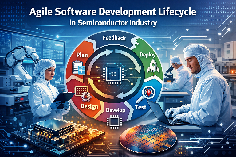
The Core Phases of the Agile SDLC for Semiconductor Manufacturing
Implementing Agile in a fab isn’t about ignoring documentation; it’s about making documentation and testing continuous.
Phase 1: Modular Backlog Grooming
Instead of a 500-page specification, requirements are broken into “User Stories.” For a fab automation engineer, a story might be: “As a tool operator, I need the SECS/GEM interface to report real-time vacuum pressure to prevent batch loss.”
Phase 2: Sprint Planning and Execution
Sprints typically last 2–4 weeks. During this time, the software team develops specific modules, such as a new alignment algorithm or a sensor calibration update.
Phase 3: Continuous Integration (CI)
Every code commit triggers an automated build. In semiconductor automation software development, this CI process must include rigorous static analysis to ensure compliance with industry safety standards.
Pro-Tip: Use “Feature Flags” to merge new code into the main branch without activating it on the production floor. This allows you to test software in the background while the tool continues to run on “Golden” code.
Implementing DevOps and CI/CD for Semiconductor Software
DevOps in the semiconductor industry is the bridge between the cleanroom and the developer’s desk. It involves automating the deployment of software to equipment globally.
CI/CD for Semiconductor Software
Continuous Integration and Continuous Deployment (CI/CD) in this sector requires a specialized pipeline. Because you cannot always “push to production” on a multi-million dollar EUV machine, the CD phase often stops at a “Staging” environment—a high-fidelity simulator or a non-production test tool.
Automated Testing and Digital Twins
To achieve a true Agile software development lifecycle in semiconductor, they are investing in digital twins. A digital twin is a software replica of the hardware. By running CI/CD scripts against a digital twin, developers can simulate thousands of wafer runs in minutes, ensuring that a new update won’t cause a mechanical collision.
Comparison: Traditional Waterfall vs. Agile for Fabs
| Feature | Waterfall | Agile (Hardware-Aware) | Best For |
| Feedback Loop | End of project (Months) | End of Sprint (2–4 Weeks) | Agile: Rapidly changing tool requirements. |
| Risk Mitigation | Heavy upfront planning | Continuous testing/Digital Twins | Agile: Preventing late-stage integration failures. |
| Documentation | Massive, static volumes | Living documentation/Auto-gen | Waterfall: Regulatory-heavy, fixed-spec projects. |
| Deployment | “Big Bang” release | Incremental updates | Agile: Fab automation and software-defined tools. |
Analysis: While Waterfall is still useful for the physical construction of a fab, the software that runs the fab must be Agile. The ability to pivot based on real-world yield data is a competitive necessity.
Expert Perspective: The Reality of “Hardware-Aware” Agile
Modern semiconductor software development is no longer just about writing code; it’s about system-level reliability. In our experience, the most successful teams don’t try to copy-paste Agile from web development. They adapt it. This means keeping the “Definition of Done” strictly tied to hardware safety. If a piece of code hasn’t been run against a safety-interlock simulator, the sprint isn’t finished. This nuance is what separates successful Agile project management for fabs from failed “move fast and break things” experiments.
Limitations: When Agile Struggles in the Cleanroom
Agile is not a silver bullet. There are specific scenarios where it requires careful handling:
- Safety-Critical Interlocks: You cannot iterate on a laser safety system in a live environment. These modules require “Mini-Waterfall” rigor within the Agile framework.
- Supplier Synchronization: If a third-party sensor manufacturer is six months behind, your Agile software team may hit a “blocker” that no amount of daily stand-ups can solve.
Legacy Toolsets: Older equipment with limited compute power may not support modern containerization or CI/CD agents.
Conclution
Agile software development lifecycle in semiconductor environments delivers faster innovation without compromising precision. By combining modular sprints, digital twins, CI/CD pipelines, and hardware-aware validation, fabs can reduce integration risks and respond quickly to evolving process demands. While safety-critical systems still require structured rigor, Agile remains essential for modern, software-defined semiconductor manufacturing success.